Maintenance notice:
These forum archives are read-only, and will be removed shortly.
Please visit our forums at their new location, https://www.evilmadscientist.com/forums/.
Howdy, Stranger!
It looks like you're new here. If you want to get involved, click one of these buttons!
Categories
- 654 All Categories
- 218 General
- 70 Ask an Evil Mad Scientist
- 6 Blog Projects
- 13 Electronics
- 16 Microcontrollers
- 10 Software Tools
- 0 Fabrication Technologies
- 436 Product Support
- 76 AxiDraw
- 26 WaterColorBot
- 172 Egg-Bot
- 2 AYAB
- 57 Clock Kits
- 23 Larson Scanner and Menorah
- 40 LED Matrix Kits
- 38 Other kit and product support
Layers of a pcb
Hi there,


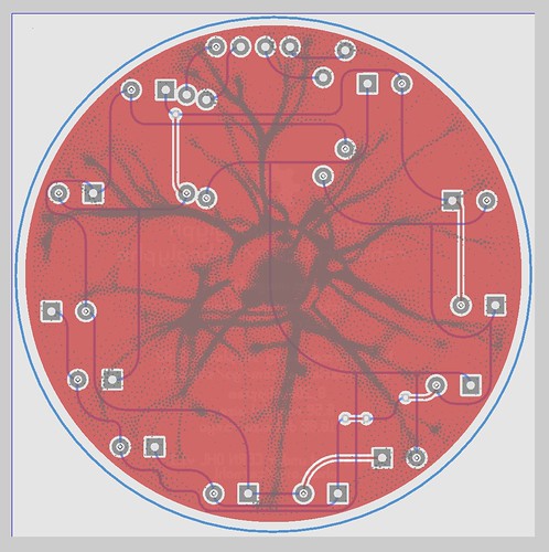
I'm trying to make a board that has some art on the 'shiny' layer (the 'pins and pads') layer in geda. The artwork appeared to be okay, and the soldermask layer was not covering it.
Here's what it looked like in geda:

Here's a pic of the soldermask layer on: http://www.flickr.com/photos/robotgrrl/7687135018/in/set-72157630843963020/
When I was having the boards made, the manufacturer said to put a fill on the top layer, otherwise it would be the pcb material that would show through. However, when I received the boards, there was no artwork showing. 
Here's a picture of the gerber, this is the top layer. From left to right is: first version without fill, second version with fill, third version with cleaned up fill.

And after the top layer, this is what is below:

Questions:
Why did it turn out the way it did?
What changes can be made to fix it (so the artwork would be shiny)?
What layer should I put the artwork on (in geda)? What layer would this be in the gerber?
Was the fill needed, or was that what caused it to mess up?
Hopefully you can help point me in the right direction at least! If it helps, you can download and look at the board from here: https://github.com/RobotGrrl/PlasmaRoboGlyph
Thanks geda guru 


Comments